Latest News


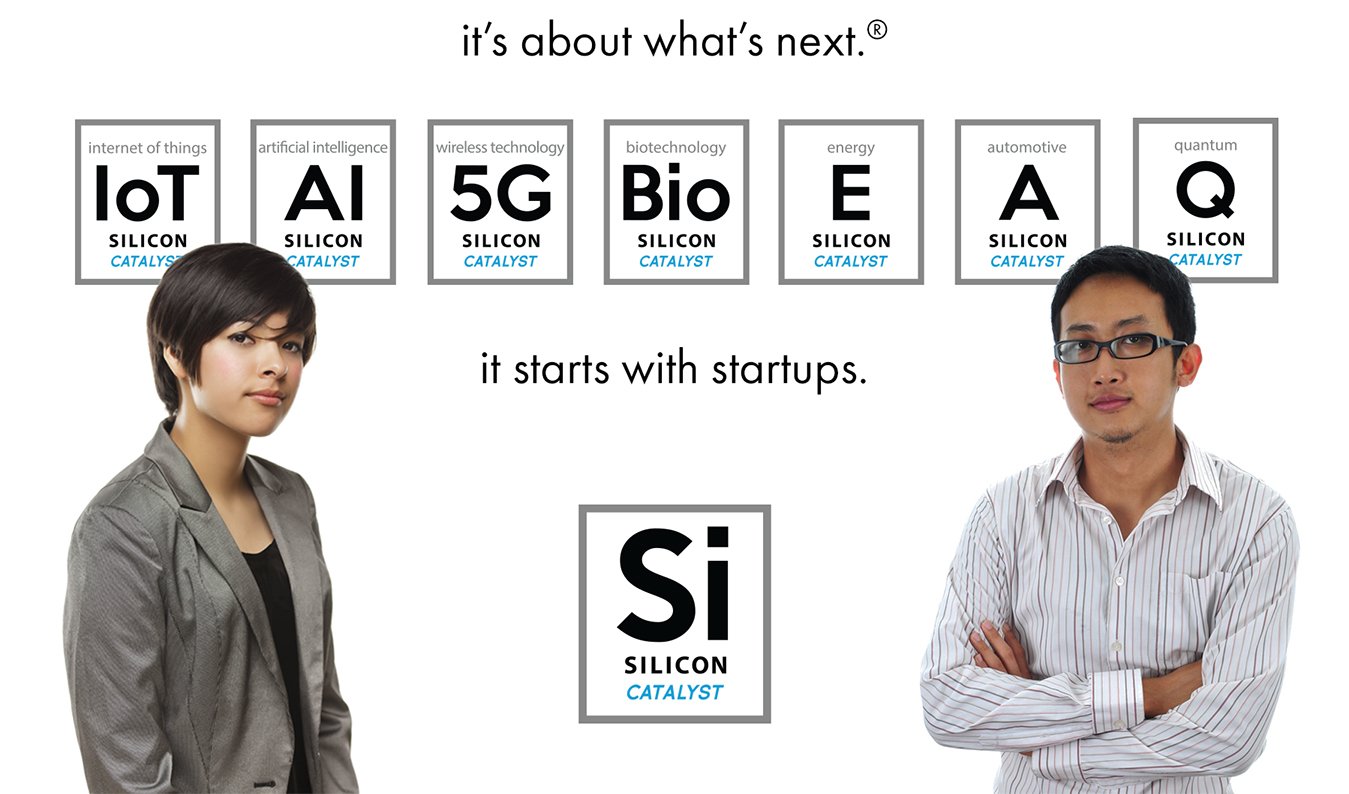
Silicon Catalyst is the only accelerator focused on the Global Semiconductor Industry including Chips, Chiplets, Materials, IP and Silicon fabrication-based Photonics, MEMS, Sensors, Life Science and Quantum.
We have engaged with more than 1,500 semiconductor startups worldwide and have admitted over 150 exciting companies. Silicon Catalyst is the Gold Standard for semiconductor acceleration. Our unique model, refined for over a decade, has been successfully franchised internationally, with global partners in the UK, EU, Israel, Japan, Australia and Malaysia.
In addition to mirroring Silicon Catalyst’s accelerator model, each of these Silicon Catalyst subsidiaries offers a ChipStart seed stage incubator which provides startup entrepreneurs direct access to Silicon Valley.
Our companies participate in a 24-month customized incubation program. Each is guided closely by a Silicon Catalyst partner. This includes a semiconductor focused curriculum and over 40 events worldwide each year. Silicon Catalyst’s ecosystem provides everything our startups need to design, fabricate, and market semiconductor solutions:
• In-Kind Partners (TSMC, Synopsys, Arm, ST, MathWorks and over 60 more) – provide each startup several millions of dollars’ worth of goods and services including EDA tools, IP, PDKs, prototypes, design and test services, packaging and business solutions. Our companies have received over $150M in in-kind goods and services.
• Strategic Partners (TI, ON Semi, Soitec, Bosch, Cirrus Logic, Arm, ST Micro, Sony, EMD Electronics, NXP, Mayfield, Qnity, GlobalFoundries and SMD Semiconductor) – participate in the selection process and actively look for opportunities to partner with our startups.
• Investors – Our partnership with Mayfield and a large group of over 500 VCs, Angels, Angel groups, Corporate VCs, and Family Offices fund each journey. Silicon Catalyst Angels, created from our ecosystem, also funds our companies. In February of 2024, Silicon Catalyst Ventures (SCV) was launched to fund early-stage startups accepted into the incubator’s two-year program. SCV has already made 26 investments in Silicon Catalyst Portfolio Companies. Our companies have received over $600M in venture investments.
• Advisors – A valuable network of over 500 industry experts that we match to the specific needs of each startup.
• Universities, Industry Organizations, Accelerators and Government Agencies – We nurture over 400 partner relationships for the benefit of our portfolio companies. Our companies have received over $100M in grants.
Silicon Catalyst’s mission is to help semiconductor startups succeed. Join us in driving innovation!
Startups start here.
it’s about what’s next.®
it’s about what’s next.®
APPLICATIONS NOW BEING ACCEPTED
Our global outreach is underway to find early-stage semiconductor startups to join our incubator.
Silicon Catalyst is the only incubator + accelerator focused on Semiconductor & Hardtech Solutions including ICs, IP, Photonics, MEMS, Sensors, Materials, Quantum and Life Science
The startups admitted since 2015 are developing innovative solutions in a variety of areas including energy harvesting, wearables, silicon photonics, memory technology, loT, high performance computing, artificial intelligence, machine learning, wireless communications, and biomedical devices.
The Silicon Catalyst incubator utilizes our coalition of in-kind and strategic partners to dramatically reduce the cost and complexity of developing semiconductor solutions. With our world-class network of mentors to advise startups, we are addressing their many challenges in moving from idea to realization and business success. We have provided our Portfolio Companies with a path to funding, free access to tools, testing and shuttle runs, along with advice on proper corporate governance and strategic execution.
Silicon Catalyst Portfolio Companies
SpiNNcloud is a deep-tech company building next-generation compute infrastructure for AI and high-performance computing.
We design the full stack, from custom silicon to supercomputer- and datacenter-scale systems. Centered on sparsity and integrated across silicon, systems, and software, our architecture is built to accelerate AI inference and deliver step-change performance and efficiency gains for HPC workloads.
As brute-force dense scaling reaches practical limits, SpiNNcloud is advancing sparsity-driven architectures capable of unlocking orders-of-magnitude improvements.
Our goal is to deliver breakthrough compute infrastructure for the next generation of AI and HPC.
S-SENTIA provides high-performance sensing solutions for optical photon and radiation detection. Its proprietary CMOS integrated sensor technology amplifies signal charge while preserving analog information with high dynamic range, enabling precise timing, pixel-level signal processing, and a favourable power-performance trade-off. The platform targets direct time-of-flight LiDAR for 3D vision in Physical AI systems, high-speed optical sensing, and radiation detection for medical and industrial markets.
Brain-CA Technologies is an innovator in microprocessor design, transforming artificial intelligence with its unique cellular automata-based processor architecture. By leveraging simple, self-contained cells operating under straightforward rules, Brain-CA's technology delivers exceptional energy efficiency, scalability, and adaptability, addressing critical challenges in AI processing such as power consumption and heat generation. With a mission to redefine AI processing for real-world applications, Brain-CA is dedicated to enabling smarter, more sustainable solutions across industries, including healthcare, finance, manufacturing, and transportation. Headquartered in Cincinnati, Ohio, and Sarasota, Florida, Brain-CA Technologies is driving the next wave of AI innovation.
VisIC Technologies was founded in 2010 with the goal of advancing Gallium Nitride (GaN) technology into mainstream usage. The initial team consisted of distinguished materials and device scientists with profound experience in technology. After a number of groundbreaking developments in materials processing and device design, resulting in a number of international patents being issued, it was decided that the technology was perfectly suited for use in the automotive industry.
The team steadily grew at company headquarters in Ness Ziona, Israel and the development effort of robust devices started. Based on the foundations of the fundamental science the development team arrived at an optimized design of one of the most reliable, high voltage, high current (650V, 100A) transistor designs. The design was neither based upon enhancement-mode GaN with its inherent gate limitations nor the restrictive performance of cascode depletion-mode GaN. The D3GaN era arrived with the novel Depletion-mode Direct Drive GaN technology emerging as an eminently suitable technology meeting the demand of highly reliable and extremely robust product needed in critical drive applications of the electric vehicle market.
VisIC Technologies works with Taiwan Semiconductor Manufacturing Company (TSMC) as a foundry source for the proprietary D3GaN process.
The company continues growing and preparing for the highly competitive, high volume automotive market adopting the relevant quality procedures and best practices for the target industry. The development hasn’t halted and new devices and modules are being designed along with novel topologies to increase performance that is demanded by the very dynamic electric vehicle market.
Today VisIC Technologies is a leader in automotive GaN products providing previously unseen levels of performance in its focused product portfolio.
Trust in over 80+ years of combined experience from our world-class development team, dedicated to delivering the highest quality and innovation in every aspect of our RISC-V microprocessor design.
Revolutionary RISC-V microprocessor architecture delivering unparalleled performance and versitility for the next generation of computing.
Scalable from 1 to 8 wide microprocessor with best in class vector processing.
Unlock Accurate Precise Lab-Quality Pathogen Results in 15 Minutes On-Site
Revolutionizing On-Site Molecular Analytics
We’re transforming pathogen detection—taking molecular analytics out of the lab and into the field.
Fast DNA/RNA Amplification & Mobile App
Our platform combines rapid DNA/RNA amplification with an intuitive mobile app, a low-cost reader, and disposable bio-cassettes to deliver lab-grade results in minutes—not days.
Versatile, Training-Free Deployment
Whether for water safety, food processing, agriculture, or biomanufacturing, our system empowers users to make faster, smarter on-site decisions—no specialized training, cold chain, or complex equipment required.

At MoRF, we are dedicated to pushing the boundaries of technology and redefining the world of RF semiconductors.
WiConnectGlobal is a driver behind NexGen’s Data centers highspeed photonic interconnects. We develop fast optical devices, with high reliability, low power consumption, and high degree of scalable economics that addresses $/Gbps, pJ/bit energy metrics, and bits/s/Hz Bandwidth expansion. Our Co-packaged solutions with hybrid integration between different technologies are essential for processing AI/ML Data traffic. The integration of electronics, photonics and packaging will deliver a state of the art solution to the industry for addressing current technical challenges. Our solution allows connections in a massive configuration for AI tailored datacenters while providing Reduced Latency, Enhanced Bandwidth, Lower Power Consumption, and Increased Scalability.
Innovate. Accelerate. Protect.
Chevin’s mission is to assure that the authenticity, origin & journey of FPGAs, ASICs and Chiplets can be verified & secured throughout each step of the silicon supply chain. Our expert Engineering Design team can assist you to achieve optimum results and security for your silicon project.
The Specialist IP Core Provider
Chevin Technology delivers high performance, configurable Ethernet IP Cores for Intel and AMD Xilinx FPGAs. Our goal is to provide reliable, hardware accelerator capabilities for high end FPGAs that are cost effective and straightforward to implement into client’s projects, using a minimum of FPGA resources. Our Ethernet IP cores are developed and comprehensively tested in-house, so we can offer valuable, expert knowledge and responsive engineering support to smooth the path for successful integration into client products.
Chevin Technology’s IP Cores achieve high throughput and sustained data rates to maximise link utilization. The compact, ‘all logic’ architecture requires no CPU/SW, therefore reducing complexity, latency and energy consumption, while leaving maximum space for further design logic on customer FPGAs. Chevin Technology’s Ethernet IP Cores also feature our patented Silicon Software Solution, which provides further design flexibility and cost efficiency, as clients have the option of adding extra features as required throughout the design cycle. Client projects include international defence; medical research, scientific research, industrial imaging, data storage.

Unveiling the Future of Diamond Technology
At Diamond Quanta, we stand at the forefront of a new era in diamond technology, dedicated to advancing the semiconductor industry with our groundbreaking work in diamond materials research. Embracing a new diamond era, our logo symbolizes our transformation of the diamond crystal space, both literally and figuratively. We're not merely a company; we're driving innovation forward, challenging the limits with our revolutionary approach to diamond electronics.
Founded in January 2024, Diamond Quanta is revolutionizing the semiconductor industry with groundbreaking diamond technology and a strategic market approach. By addressing both technical barriers and economic realities, we position ourselves as key players in high-value applications of electronic and quantum technologies. Our team, comprised of highly skilled professionals with decades of experience in advanced diamond and nanocarbon materials, excels in electronic, photonic, and optical-mechanical device development. We have a proven track record of transforming laboratory innovations into real-world solutions for leading semiconductor, aerospace defense, and consumer electronics companies, driving the industry toward a smarter future.
WHAT WE DO
TeraSpatial is building wireless communications and networking solutions comprising silicon, software and deeply embedded AI/ML to solve the connectivity bottleneck for AI data movement.
Our Unique Wireless Connectivity Offering Combines
Two Patented Technologies
The limitations of traditional networks
As GenAI is deployed across distributed and edge infrastructures, or where rapid deployment is needed, or where endpoints are not stationary, traditional connectivity will not meet the needs of high data rate use cases such as training, visualization, and digital twin.
The TeraSpatial Advantage: 10X Wireless Capacity
TeraSpatial’s connectivity solution uniquely solves this problem by delivering 10X wireless capacity compared to existing solutions, at 10X lower cost than deploying fiber.
Providing Connectivity for the Growing GenAI Market
Target customers include network/IT equipment providers for the infrastructure, enterprise, industrial, and government/defense segments, where GenAI is driving explosive demand for high-speed, low-latency data transport networks to disseminate data from physical interfaces to points of computation.
About Blacksol Nanotech
Our team have more than 10 years experience in nanotechnology. The first step is lower the cost of carbon nanomaterial to become affordable. Then, designing and assembling carbon materials into right structure for applications are important to help our customer to solve problem. Last, we are the expert of carbon product manufacture, including film, polymer composite, coating, paste, powder,... Currently, we focus on carbon nanocomposite. The extraordinary properties of metamaterial reveal a new chapter of the application of carbon nanomaterials. In the following generation of 5G, 6G, high speed data transmission, AR/VR, wearable device, stealth technology, Blacksol nanotech is seeking for cooperation partner to make the future better.
Gigantor Technologies
Giants of Neural Network Acceleration
At Gigantor, we are not just another tech company but pioneers, innovators, and trailblazers.
Our customers rely on our commitment to innovation and proprietary circuit designs that are redefining the Edge AI's landscape. Our cutting-edge technology ensures seamless real-time operation, enabling AI to handle ultra-high resolutions and high frame rates without compromising a single frame. Our systems are meticulously crafted to embody power efficiency at their core.
In the beginning...
Founded in 2020, Gigantor Technologies was born out of a shared vision to redefine the boundaries of AI and neural networks.
Our co-founders, passionate tech enthusiasts, were not content with the status quo. They saw the limitations of Edge AI — the inability to process in real-time, dropping frames, struggling with high resolutions and frame rates, latency issues, and high power consumption.
Their unwavering determination and groundbreaking ideas led to the development of our patented technology, which has since transformed the face of Edge AI.
HEPT Lab is developing a fully solid-state, coherent 3D image sensor, the size of an Apple Airpod case, to enable autonomous devices. Our solution is resilient to harsh conditions such as bright light, dust and fog, critical for Automotive, Agtech, Robotics and Drone markets. Equally important for these markets are small size, low power and low cost. HEPT Lab’s solution combines three classes of in-house designed semiconductor devices assembled into one multi-chiplet sensor solution to achieve these requirements. A custom silicon photonic ASIC implements solid-state beam steering and coherent imaging architecture, multiple analog CMOS devices interface with the silicon photonic core and a custom InP photonic ASIC generates and conditions the laser signal.
We make Wi-Fi. Better.
Edgewater Wireless is a leading provider of innovative spectrum slicing technology for residential and commercial markets. With a focus on high-density and high-quality service needs, Edgewater Wireless develops advanced Wi-Fi silicon solutions, access points and IP licensing. With over 26 granted patents, Edgewater Wireless continues to revolutionize Wi-Fi, making it better for everyone.
Edgewater’s physical-layer spectrum slicing allows a frequency band to be divided or sliced to enable more radios to operate in a given area. Think of spectrum slicing like moving from a single-lane road to a multilane highway — regardless of Wi-Fi technology. The recently completed proof of concept (PoC) with a major Tier 1 service provider showed seven to 18 times performance gains in 75 per cent of homes surveyed. Interestingly, homes with the most devices saw the greatest improvements.
Jmem Tek Launched the World’s First PUF Based Post-Quantum Cryptography (PQC) Chip.
As part of the upstream semiconductor industry, Jmem Tek specializes in hardware security IP and provides IC design services, focusing on next-generation hardware security solutions that defend against hackers while ensuring data protection.
With the rapid advancements in quantum computing, global attention is increasingly focused on post-quantum cryptography (PQC) and the high-risk cybersecurity issues associated with data leakage, counterfeit chips, identity theft, and algorithm tampering. There’s an urgent need for solutions to prevent the growing threat of cyberattacks. Research indicates that a cybersecurity incident occurs every 37 seconds, and by 2028, the cybersecurity market is expected to reach $290 billion.
The best solution lies in hardware. Jmem Tek integrates security directly into chips, creating comprehensive hardware security modules and an invisible key. Our solutions protect chips from illegal duplication, ensure secure identity authentication, offering post-quantum cryptographic encryption algorithms that even quantum computers cannot break, safeguarding data from all potential threats.
RED Semiconductor is developing technology to solve three hard problems
“Software gets bigger more rapidly than microprocessors get faster.” Complex AI, cryptography and analytical algorithms have fundamentally changed data processing requirements. Traditional architectures are no longer ideal for today’s processing applications.
“Reducing silicon geometries no longer drives enough performance increase.” The only way to boost processor performance is to re-think fundamental architectures.
“Global legislation enforces everybody’s right to privacy and security of data.”. Processors must protect privacy and enable safety.
CrossFire Technologies Inc. is solving the AI to Memory Bottleneck with its patented Bridging Chiplet (Bridgelet™) Products and Direct Chiplet Interface™ (DCI) Intellectual Property. CrossFire’s solutions unleash memory bounded compute while reducing the energy required to transfer data between compute and memory.
MSM is developing an innovative Dynamic Random-Access Memory (DRAM) addressing the limitations of current memory technologies. MSM DRAM is based on multi-level cells (MLC) enabling higher bits density, better power efficiency and silicon scalability, making it ideally suited for demanding applications such as artificial intelligence, high-performance computing, and mobile devices.
Our mission
Hardware building blocks that break barriers
Backscatter technology allows devices to send more data for way less power, cost, and size, unlocking engineering imagination.
Power consumption of conventional radios constrains engineers and product designers. WaveWorks' technology enables the same standard protocols with up to 99.9% less power.
Introducing Ultra Edge® circuit-level artificial intelligence. Transforming the smart technologies and processes driving our world.
Ultra Edge® technology, redefines a new era of circuit design, enabling predictive maintenance and improved performance of every closed-loop control system.
'wee'
[wee]
adjective [Scottish] we·er, we·est.
little, very small, tiny
weeteq is an innovative Scottish company developing tiny technology that revolutionises Global industries. Our executive team have collectively spent over 50 years in deep tech and smart technology businesses, working for some of the world’s most respected tech companies.
We partner with other smart technology manufacturers and operators to deliver our mission of developing circuit-level artificial intelligence solutions to accelerate the sustainable growth of the smart technologies and processes driving our world.

High Frequency Radar
We have developed a new solid-state high-frequency radar imaging technology. Reducing the size and cost while improving the performance. Our radar can see through fabrics, plastics and cardboard while running at video frame rates in a portable form factor.
We spun out of MIT after developing breakthroughs in THz imaging radar, building numerous antennas onto a size smaller than a credit card. This enabled us to demonstrate the first solid-state imaging radar at 300 GHz.
The 300GHz operating frequency and solid-state beam forming give us superpowers, enabling never-before applications.
The electromagnetic energy efficiently transmits through fabrics, plastics, paper and cardboard. Allowing us to see and measure in 3D what is concealed under clothing, or what is inside cardboard boxes.
The solid-state beam forming means we can steer the beam with sub-degree accuracy, making our radar more like a cellphone camera than a traditional radar, with high image resolution, low power and portability.
Alumni
RAAAM provides the highest-density embedded memory in standard CMOS
developed a unique on-chip memory technology which offers the highest-density embedded memory in a standard CMOS process, requiring no additional process steps or cost.
technology provides up-to 50% smaller memory footprint compared to the highest-density commercial solutions based on 6T SRAM.
memory IP which can be used as a drop-in replacement for SRAM,
offering a significant cost reduction, improved bandwidth, and reduced power consumption.
patented technology has already been proven in silicon with multiple test-chips of leading semiconductor foundries (e.g., TSMC, Samsung, ST Micro).

What we do
At ABR we develop new kinds of AI that exploit temporal neural networks. Our algorithms and the hardware we use ranges from the conventional (CPUs, GPUs, deep networks, ANNs) to the unconventional (spiking ASICs, FPGAs, adaptive controllers, SNNs). We have deep expertise in using neuromorphic (and standard) hardware and software to solve AI problems. We have developed a software platform, Nengo, that flexibly combines all these methods to get you the lowest power, fastest speeds, and highest accuracy.
OUR VISION
-Overhauling Decades of Light Emitting Diode (LED) Display Technology-
Since the invention of the first light-emitting diode (LED) over a century ago, solid-state lighting technology has since become ubiquitous, from home and commercial lighting, to various display technologies. MicroLEDs (LEDs < 100 μm), are the sought-after Holy Grail of the display industry due to their improved energy efficiency, faster response time, and higher pixel density, which lend to superior display resolution and performance compared to the MiniLED (LEDs >100 μm) technology of the past few decades. Moreover, the current manufacturing practice of selectively placing millions of tiny RGB LEDs is an extremely challenging and cost-prohibitive process.
As a stealth startup, we have developed a series of innovations that revolutionize microLED technology, from material growth to device fabrication and assembly. These novel approaches are based on our core technology: the polychromatic RGB microLED. Our polychromatic LED is a revolutionary device which replaces the century-old monochromatic LED, and promises to solve several key issues with decade-old microLED display technology.
At Q-Pixel we aim to overcome the obstacle of high fabrication costs and to dramatically streamline the LED display assembly processes. Our objective is not only to significantly reduce the cost, but also to minimize the number of defective pixels and maximize assembly speed for high-yield, high-throughput, foldable large area (>100 inch) microLED displays. Notably, our technology is also entirely transferrable to smaller displays, such as mobile phones, tablets, personal computers, and wearable devices (Smartwatches/AR/VR).
Please wait and see what Q-Pixel can do for the display industry!
Zero-power sensors with uninterrupted operation and unprecedented accuracy.
Pinnacle Semiconductor, Inc., is a Silicon Valley Semiconductor Company that invented and patented SCMOSTM, a fundamental circuit technology delivering SoC designers a quantum leap in power, performance, and area (PPA), for both logic and embedded memory. Pinnacle offers its customers all the advantages of the NEXT NODE, NOW.
Ainekko is a startup building the first open, software-defined platform for AI infrastructure—extending open-source principles all the way down to silicon. By offering flexible, modular hardware and tooling, Ainekko empowers developers to build efficient, composable AI systems for edge and data center applications alike. Founded by industry veterans with deep expertise in open systems and silicon design, Ainekko is on a mission to make AI hardware accessible, developer-driven, and community-powered.
Science and Technology of Digital Agriculture
We are passionate about the food we eat, and how we can improve it through Geegah technology. We are dedicated to providing the devices and systems that free up the human mind to do fun and creative things without worrying about our food. We are developing technologies for Internet-of-Plants, being able to image soil and provide real time data on plant health, through our partners at ARPA-E and the The Bill and Melinda Gates Foundation.
State-of-Art Biometric Sensors
Making electronic payments securely effects us all to feel safe in a world full of fraudulent intent. At our company, we are developing most advanced sensors to offer the most secure and convenient biometric sensors. Based on gigahertz (Hence, the name GEEGAH) ultrasonics we offer single chip biometric solutions with an emphasis on fingerprint sensing.
Quantum Power Transformation (QPT) is a revolutionary start-up with a vision to help the world save energy through the development of unique IP that can revolutionise power electronics systems, radically improving efficiency & performance.
These benefit almost any consumer or industrial based electronic system; reducing power consumption, increasing efficiency and the reliability of power systems. Applications include ac:dc converters, dc:dc converters, inverters and electric motor control systems.
Rune’s CC/CS™ data center helps solar and wind power plants address the multi-billion dollar problem of value deflation, clipping, and curtailment.
[Step 1] Rune installs CC/CS™ data centers behind-the-inverter at a solar or wind plant’s DC bus bar and doesn’t need AC supply from the grid
[Step 2] Rune autonomously determines availability of stranded and surplus power, and sends to CC/CS™ data center
[Step 3] Rune CC/CS™ data center generates revenue by performing interruptible computational workloads and power producer monetizes otherwise unmarketable power
Consumer Devices
Capacitive Imaging from SigmaSense enables OEMs and ODMs to be first to market the most intuitive, robust and innovative products to consumers.
Large Format Interactive Displays
Fully scalable. Digital. Environmentally resilient. Introducing the next evolution in Large Format Interactive Display capabilities.
Custom Implementations
SigmaSense Sigma-delta Architecture will traverse industries, environments and form factors with virtually limitless potential in application.
Artificial Intelligence is here, not only to stay, but to change our world. A long time ago Humans invented the wheel to move faster and to help relieve their muscles from heavy jobs. Today, we humans are shaping and developing the AI, to help our most important muscle, the brain, to go further and open new unthinkable landscapes, new opportunities and new jobs. Mentium has the technology to bring ultra-fast AI to low power electronics, like cameras, sensors, microphones, wearable accessories, and bring the performances of autonomous vehicles and AI cloud computing to a whole new level.
Our architecture is based on Non-Volatile Memory devices used to carry out analog in-memory computation, eliminating the memory transfer bottleneck and exploiting the inherent efficiency of analog computation. Analog computing is an old concept abandoned a long time ago due to its troubles dealing with variations and noise, leading to low precision computation. Mentium Technologies Inc. solved these issues and our technology showed incredible resilience to temperature and device variations: we are able to deliver extremely fast and efficient AI computation.
Lelantos is revolutionizing the world of gas sensing by developing a new generation of IoT compatible gas sensors targeted to high value monitoring applications in threat detection, industrial safety, environmental and air quality monitoring as well as medical diagnostics. Current gas sensors are based on optical and resistive technologies and suffer from inherent weaknesses such bulky size, high power consumption and high cost. As such they prohibit the effective monitoring in IoT oriented use cases that require large scale, pervasive sensing to be provided by autonomous, portable, battery operated sensors with wireless connectivity. In contrast, Lelantos sensors based on CMOS integrated piezoelectric resonator arrays can achieve up to 1000 times more compact size, lower power consumption and lower cost than currently utilized systems. As a foundationally superior sensing technology, Lelantos is enabling the widespread adoption of gas sensing in IoT applications and the disruption of the market providing a true chemical sensor for the Internet of Things.
OUR TECHNOLOGY
At Lemurian, our goal is to make deep learning affordable and available for everyone, from the individual researcher to industry.
The Lemurian SPU (Spatial Processing Unit) is more than an order of magnitude more efficient in terms of memory and power in comparison with legacy processors, whilst also being faster in inference.
Our processor makes use of a novel digital arithmetic which has been designed specifically in order to speed up matrix-vector multiplications which largely make up modern deep neural networks, whilst also reducing hardware complexity.
Our arithmetic and processor architecture results in tremendous power and memory savings, thereby making our processor more affordable and well suited to inference at the edge.
Espre Technologies is an innovative solutions provider developing technologies related to next generation wireless products. The company holds intellectual property related to Internet of Things (IoT) for 5G networks and embedded cooperative network solutions, carrier aggregation techniques in LTE, and A.I. applications related to real-time user wireless data capture and analytics. Espre has developed and patented an industry disruptive communications protocol that is designed to integrate within existing WiFi and cellular networks.
Espre was founded by Dr. John Terry, a recognized industry expert in wireless communication system design in the areas of chaos communications, WLAN & OFDM networks, and carrier aggregation for LTE and WiFi networks. Dr. Terry has generated over 50 issued / pending domestic and foreign patents related to wireless technology. Further company information can be found at www.espretech.com
Enabling edge intelligence
We offer highly scalable and rapidly customizable energy-efficient AI accelerators for the extreme edge applications such hearing aids, wearables, bio-medical monitoring, AR/VR and others.
Our goal is to enable the next generation of edge devices that are an order of magnitude smarter than they are today.
Adaptiva is a neural network accelerator that delivers between 10 to 100 TOp/s/W of energy efficiency. We seek to enable the next generations of smart edge devices.
What is possible today
Basic activity detection
Face Identification
Keyword spotting
We enable more
Speaker isolation
Precise activity recognition
Emotion recognition
Visual odometry
Speech synthesis
&
many others...
NanoHydroChem is an advanced materials company developing and commercializing nanomaterials for energy storage applications.
Phinomics uses circular DNA, an early marker of genetic and environmental change, to diagnose disease and radically improve human health. By isolating and sequencing the circular genome ("the circulome", a term we coined), we solve a genetic puzzle that unlocks a universal “stage-zero” diagnostic for disease. At scale, circulome data will revolutionize diagnostics and identify new therapies.
Oculi makes the SPU™ Sensing and Processing Unit, a complete edge vision system on a chip, that overcomes power, bandwidth and latency constraints. The Oculi SPU is a high performance, edge processing, low latency, low bandwidth, high speed sensor, and is an ideal solution to scale an intelligent network over a wide area for use cases in traffic monitoring, analytics and tolling. Oculi is deployed on a US public highway and partnering with various companies to deliver innovative solutions to market.
Salience Labs is building a hybrid photonic-electronic chip for AI. We have designed a massively parallel, ultra-high throughput Photonic Tensor Processing Unit. Photonics allows data to be modulated at up to 100 GHZ, and allows for high levels of parallelization using multiplexing. We integrate this photonic unit into a SoC architecture designed to exploit its high throughput for AI inference. Salience Labs technology is based on decades of research collaboration between Oxford University and University of Münster, Germany.
Sonical is revolutionizing the way we hear. In the same way you use apps on your phone, Sonical is putting apps in your ears. To make this possible we are designing and building the world’s first ear computer that has the capabilities and performance for next generation ear worn products. To make our intuitive platform accessible we are creating EarOS to unlock thousands of existing and new developers. Our ear worn solutions will enable everyone to have a personalized hearing experience and to control how they hear the world using AI and advanced audio processing.
Quadric believes the road to an autonomous future must be completely re-architected. As the need for speed becomes more important than ever for millisecond decision-making in machines, data doesn’t have time to go round-trip to the cloud. Advanced edge computing is the answer, but requires a start-from-scratch approach. By combining high performance computing with the most sophisticated artificial intelligence, Quadric’s technology is helping to realize the promise of the future: where cars will finally commute safely for us, where industrial robots will complete critical tasks, where humans will communicate with machines like never before.
Your processor needs a bodyguard.
Dover Microsystems’ CoreGuard® technology is the only solution for embedded systems that prevents the exploitation of software vulnerabilities and immunizes processors against entire classes of network-based attacks.
Forget Everything You Know About Cybersecurity
On average, all complex software contains up to 50 bugs per 1,000 lines of code. So, it’s no surprise that nearly every cyberattack relies on exploiting a software vulnerability. Today’s cybersecurity solutions focus on building defensive software around networks and applications to protect our embedded systems. Rather than securing the system, this approach actually increases a system’s vulnerability by adding yet another layer of inherently flawed software. As a result, companies and individuals are left even more exposed.
Compact 60 GHz Radio for Wireless Backhaul
MICROHORN PHASED-ARRAY ANTENNA
The phased array antenna automatically scans and locks onto the strongest signal by electromagnetically shaping and steering the beam. There are no moving parts.
GIGABIT THROUGHPUT
Full bi-directional throughput at gigabit data rates.
60 GHz Wireless Transceiver
COMPACT SIZE
The small antenna size (4 cm x 2.5 cm) is unobtrusive and perfectly suited for mounting in an urban environment.
RANGE TARGET
Support for distances up to several hundred meters.

mmTron is the world’s leading provider of innovative mmwave linear power efficient broadband products. Our focus is on high-growth segments of mmwave markets: 5G, 6G, instrumentation, defense, satellite and aerospace communications.
We work with world-class MMIC foundries and collaborate with our customers to deliver superior products, outstanding technical support and uncompromising customer service.
Ayar Labs helps companies keep up with skyrocketing volumes of data by miniaturizing fiber optic transceivers and making them in silicon chips, bringing the super-high bandwidths and low energy use of fiber optics inside computers.
Eridan Communications is a fabless technology company developing the devices and firmware for the next generation of communications hardware for 5G and beyond. We’re based in Silicon Valley, but we leverage technology partners and resources from around the world.
Owl Autonomous Imaging has recently completed and delivered a two-color infrared camera for the US Air Force. Leveraging this technology and the associated patent portfolio, Owl AI is now developing a 4D-camera that combines 1550nm Flash-LiDAR and Thermal imaging (IR) within a single solid-state mega-pixel focal plane, targeting ADAS and Autonomous vehicles. This is a unique sensor fusion solution for the industry.
Owl AI was co-founded by Chuck Gershman. Mr. Gershman has 30 years of semiconductor industry experience in executive management, marketing, engineering, business development, sales, consulting and executive advising. A serial entrepreneur, Mr. Gershman has been a member of the executive team of five startups, three of which as CEO/COO. He has had successful exits with acquisitions by Intel and PMC-Sierra. Further company information can be found at www.owlai.us
Today there is an ever-increasing demand for portable devices with extended battery life as well as greater performance. However, the supply is being limited by the efficiency of the processors and displays that comprise two of the largest energy consumers within those portable devices.
In response to the power-efficiency dilemma facing manufacturers of portable consumer electronics, Power Down Semiconductor developed Low Power Processing (or LPP™). The technology uses a “pseudo-adiabatic” technique to recycle charge and prevent CV2f losses in memory blocks, clock buffers, GPIO, and displays.
SPARK is the enabling wireless technology of the future. Its efficiency, agility and robustness allow it to address a large number of markets, many of which are ill-served by current wireless technologies. The SPARK Radio is a wireless transceiver that is more effective than any existing technology, increasing the energy efficiency of wireless communication and enhancing battery life. This is made possible by a unique architecture that provides an order of magnitude better energy efficiency than the state-of-the-art, and this improvement is achieved through key circuit and system level innovations. Our goal is to significantly extend the limited battery life of electronics that require short-range wireless communications, as well as to increase the robustness and agility of their wireless links.
Probius Diagnostics is developing an application-agnostic, embedded point-of-care (PoC) diagnostic.
The agnostic, broad-spectrum nature of our solution makes it reconfigurable for assays of proteins without the need for specific probe or label. This is unprecedented and very compelling for a wide range of PoC applications, such as rapid screening in urgent care settings, clinical trials for pharmaceutical research, ambulatory endocrine response monitoring in chronic diseases and personalized therapeutics, as well as in-field diagnostics for biothreats and food/water quality monitoring.
One Silicon Chip Photonics’ (OSCP’s) mission is to produce simple, light, low-cost, low-power, high-performance Micro-Opto-Electro-Mechanical Systems (MOEMS) components and integrate them on Silicon-On-Insulator (SOI) substrates to create sensors for different applications, in particular motion sensors to measure acceleration or rotation of an object.
The EdgeOps™ platform is highly scalable and adaptable
– Edge Intelligent Operations platform
– Unpackage autonomous functionality
– Improve efficiency of operational equipment
– Introduce self-adaptive automation systems
– Predictive Analytics integrated with OT data
– Increase availability with self-adaptive functionality
Active Layer Parametrics (ALP Inc.) has developed a system to rapidly and accurately measure mobility and activated carrier concentration profiles with Angstrom-level resolution for the semiconductor manufacturing industry. These profiles detail the depth of electrical activation due to implant-anneal recipes. We're the only system in the world that is capable of doing these measurements on a routine basis. The goal of the company is: Improve Yield by Quick Feedback: Instead having to wait for weeks to get devices made, we could do that in a matter of minutes. Improve Device performance: By tracking process changes to electronic impact - we currently do this 'matrix-analysis'.
Zeno Semiconductor, Inc. develops and licenses novel memory and logic technologies, which provide innovative paths to scaling semiconductor devices. The memory and logic technologies are manufacturable on mainstream CMOS and FinFET fabrication processes, with no new materials or equipments, with no changes to any of the existing libraries and IPs. Zeno currently has been awarded more than 50 patents.
WHAT IS POLYN TECHNOLOGY?
THE WINNING BLEND OF ACADEMIA POWER OF MIND AND INDUSTRY EXPERTISE
POLYN Technology is a fabless semiconductor company with teams located in Israel, UK, USA, and France.
The Company’s unique NASP technology provides fast and easy conversion of trained Neural Networks into Tiny AI silicon chips with ultra-low power consumption, low latency and small size. NASP is Neuromorphic Analog Signal Processing of raw sensor data of any type.
NASP can be highly tailored for any specific application and yet affordable for mass market.
Within the lines of a fingerprint is the roadmap that makes each one of us unique. At EXOKĒRYX, our roadmap to transforming early disease detection combines principles from the semiconductor industry with breakthrough biotechnology.
Exosomes are crucial to cellular communication within our bodies and hold the key to early cancer detection.
EXOKĒRYX is revolutionizing early-stage cancer diagnostics by combining the power of solid-state electronics with exosome-based biomarker discovery.
We are developing a novel chip-based platform that leverages the dipole moments of exosomes to isolate, and transistor technology to quantify and analyze them in biological fluids to create your CancerFingerprintTM.
From a few drops of biological fluid, we can identify biomarkers with greater sensitivity than standard methods. This level of sensitivity allows for the detection of cancer and other serious disease earlier than is possible with current technologies.
Meaning we can extend quality of life by avoiding therapy pathways that are as harmful as the disease itself.
It’s time to usher in the new next generation technology.
It’s time to put our fingerprint on positive patient outcomes.

4K-MEMS SA is developing game-changing micro NIR/SWIR sources for machine vision, hyperspectral imaging, and embedded spectroscopy. Covering the 0.8-to-5 micro wavelength range, these emitters are designed for deep integration into embedded analysis modules, meeting the growing demand for high-quality broadband infrared sources. Founded on the principle that technology should be elegant and accessible, the 4K-MEMS emitters enable chip-scale infrared analysis that will revolutionize markets including individualized food quality analysis, personalized health monitoring, and machine vision.
UV-curable metal oxide thin films
Phosio is developing UV-curable metal oxide thin films, allowing deposition at ultra-low temperatures (as low as 150°C) - a significant improvement over sol-gel methods. PhosioLux® products are compatible with various solution-based deposition techniques, such as spin coating, slot die coating, and ink jetting, enabling rapid deposition at a lower cost compared to vapor deposition methods. PhosioLux® products can be patterned with direct UV exposure or techniques like nanoimprint lithography. This platform technology finds applications in transistors, OLEDs, MicroLED, and AR/VR devices.
Enabling The Convergence of Sensing and Communications
Microelectronics for Critical Systems
We develop high performance microelectronic components to enable the secure collection, processing, and distribution of critical data.
About Niobium Microsystems
Niobium builds upon decades of commercial and federal cryptography and system-on-chip expertise. Our team has completed 7 tape-outs leading to production of both commercial and custom military silicon in the areas of
high-speed crypto, phased array, AI/ML, side channel resistant chips, ultra low power.

Harness the Power of Light for AI
At Neurophos, we pioneer a revolutionary approach to AI computation, leveraging the vast potential of light. Our cutting-edge technology, powered by optical metasurfaces and silicon photonics, introduces a new era of ultra-fast, high-density AI inference that outstrips the capabilities of traditional silicon photonics.
Silicon Photonics: Speed Is Key
While our metasurface ensures high density, we haven't compromised on speed. We integrate high-speed silicon photonics to feed our metasurface in-memory processor, leveraging its high modulation speeds. The result is a fast, efficient vector-matrix multiplication engine that combines the density of the metasurface with the velocity of silicon photonics modulators.
High-Density Metasurface: Size Matters
Our metasurface elements function as optical in-memory compute elements that are thousands of times smaller than traditional silicon photonics modulators, allowing our architecture to process vastly larger matrices on chip. This results in an unprecedented increase in the computational density that provides a major advantage over conventional silicon photonics. In optical computing, energy efficiency is proportional to array size, so our processor is hundreds of times more efficient than the state of the art.
The Neurophos Advantage
At Neurophos, our mission is to deliver AI computation solutions that are not just faster, but more efficient and denser. Our unique approach combines the best of optical metasurfaces and silicon photonics, offering an AI inference acceleration solution that is poised to reshape the AI landscape. Join us as we light the way to the future of AI.